
Рефераты по рекламе
Рефераты по физике
Рефераты по философии
Рефераты по финансам
Рефераты по химии
Рефераты по хозяйственному праву
Рефераты по цифровым устройствам
Рефераты по экологическому праву
Рефераты по экономико-математическому моделированию
Рефераты по экономической географии
Рефераты по экономической теории
Рефераты по этике
Рефераты по юриспруденции
Рефераты по языковедению
Рефераты по юридическим наукам
Рефераты по истории
Рефераты по компьютерным наукам
Рефераты по медицинским наукам
Рефераты по финансовым наукам
Рефераты по управленческим наукам
психология педагогика
Промышленность производство
Биология и химия
Языкознание филология
Издательское дело и полиграфия
Рефераты по краеведению и этнографии
Рефераты по религии и мифологии
Рефераты по медицине
Курсовая работа: Bipolar transistors
Курсовая работа: Bipolar transistors
6. Bipolar transistors
6.1. Device, constructive technological features, circuit of insert
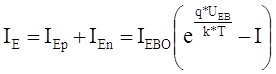
The bipolar transistor terms a three-electrode semiconductor device with two or more interacting electron-hole junction. In the transistor alternate as an electrical conductivity three regions of a semi-conductor, for what in a homogeneous semi-insulating substrate of silicon Si-i the methods of epiplanar technique shape regions of a collector, basis and emitter, (fig. 6.1). For it in a plate Si-n, employee by a collector, the method of a local diffusion (introduction of atoms of doping substance in a chip of a semi-conductor through some part of its surface) forms base region (Si-p). In this region also method of a local diffusion forms emitter region (Si-n) with high density of a donor dopant. On boundary region of emitter with base, and also on boundary of base region with collector are formed two electron-hole (p-n) junctions - emitter and collector (on a title of extreme regions of transistor structure).
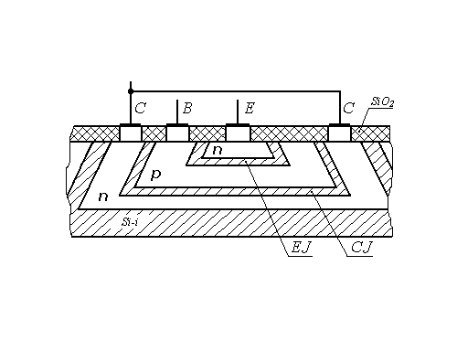
Fig. 6.1. Planar n-p-n structure of the bipolar transistor
The junctions appear
interacting, if distance between them, called in breadth of basis ![]() , is smaller diffusion
lengths of mobile carriers of a charge. The diffusion length
, is smaller diffusion
lengths of mobile carriers of a charge. The diffusion length ![]() is a distance, which
transits an electron and vacant electron site from a moment of occurrence in a
semi-conductor up to a moment of a recombination
is a distance, which
transits an electron and vacant electron site from a moment of occurrence in a
semi-conductor up to a moment of a recombination ![]() .
.
The area of collector junction always is more than the area of emitter junction. The region of the emitter should have higher electrical conductivity, than basis and collector. An impurity concentration in the region of the transistor owe corresponds as:
![]() .
(6.1)
.
(6.1)
Depending on the order of alternation of regions as an electrical conductivity distinguish structures p-n-p and n-p-n of types.
In a fig. 6.2 the structures p-n-p and n-p-n and their legend on circuitries are shown.
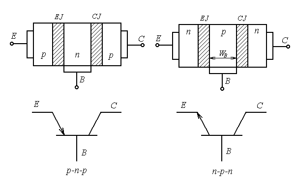
Fig. 6.2. Flat one-dimensional model BT and legends
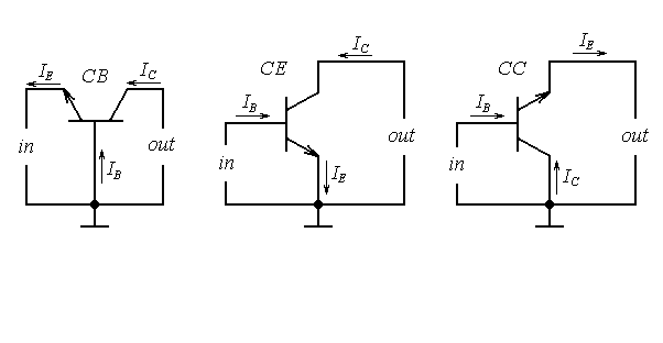
Fig. 6.3. The circuits of insert of bipolar transistors
As a device of an electric circuit, transistor use by such fashion, that one of its electrodes is entering, and another-output. The third electrode is common concerning an input and exit. Depending on what electrode is common, distinguish three circuits of insert of the transistor: common-base (CB), common emitter (CE) and common collector (CC) (fig. 6.3).
6.2. Conditions of insert of the transistor. Static parameters.
Physical processes
By operation of the transistor the voltages from exterior power supplys are affixed to its electrodes. Depending on polarity voltages affixed to electrodes, each of p-n-junctions the transistor can be switched on in direct or in the opposite direction. Four conditions of insert of the transistor are possible.
The table 6.1
| Title of junction |
Insert of junction |
A title of a condition of insert of the transistor |
|
EJ CJ |
Backward Backward |
Condition a splitting contact |
|
EJ CJ |
Direct Direct |
Condition of saturation |
|
EJ CJ |
Direct Backward |
Fissile condition |
|
EJ CJ |
Backward Direct |
Inverse condition |
1. Condition a splitting contact. In a condition a splitting contact both p-n- junction are backswitched on (high-ohmic state of a section E-C). In electrodes of the transistor the thermal currents backswitched of junctions flow past which are static parameters of a condition the splitting contact. In each of three circuits of insert of the transistor these parameters have particular magnitudes. Their labels look like
for the circuit
with CB - ![]() ;
;
for the circuit
with CE - ![]() ;
;
for the circuit
with CC - ![]() ,
,
where the first index means an electrode, in which the current flows past;
the second index – circuit of insert;
the third index - requirement in the rest of the circuit:
о - absence of a current in the other electrode - no-load operation,
s - short-circuit in the rest of the circuit.
2. Condition of saturation. In a condition of saturation both p-n-junctions are directly switched on, the junctions saturated with mobile carriers of a charge, their resistances are small. The section E-C has high conductance and it is possible to consider it short-circuited.
Static parameters are the
saturation currents in electrodes the transistor ![]() and
residual voltages
and
residual voltages ![]() . A voltage ratio
and currents relevant electrodes give magnitudes of resistances of saturation:
. A voltage ratio
and currents relevant electrodes give magnitudes of resistances of saturation:
 ;
; 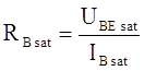 .
.
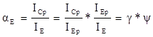
3. Fissile condition. In a fig. 6.4 the flat one-dimensional model of the transistor is shown, which emitter junction is switched on in a forward direction, and collector junction - in backward. Such insert corresponds to a fissile condition, and the transistor has intensifying properties. The principle of operation of the transistor in a fissile condition grounded on use of the following phenomena:
- injection of majority carriers through emitter junction;
- transport of injected carriers through basis owing to diffusions and drift;
- recombination of nonequilibrium carriers in basis;
- extractions of carriers from basis in a collector by a region of collector junction.
The injection of carriers
stipulates transiting through emitter p-n-junction of diffusive currents: hole ![]() and electronic
and electronic ![]() .
.
In an external circuit of emitter the current of injection flows past
 ,
(6.2)
,
(6.2)
where ![]() - hole current of
injection of the emitter;
- hole current of
injection of the emitter;
![]() - electronic current of
injection of the emitter.
- electronic current of
injection of the emitter.
For transistor structure
p-n-p of a type the relation between admixtures in the emitter and basis is
defined, as:![]() . Therefore
. Therefore ![]() .
.
The relation between component of an emitter current is evaluated coefficient of injection
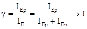 (6.3)
(6.3)
The injection of carriers from the emitter in basis rises density
minority carriers in basis. Their density on boundary of emitter junction for p-n-p of structure is defined by a relation
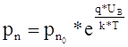 (6.4)
(6.4)
Appeared near to emitter
junction in basis a charge of vacant electron sites almost instantaneous,
during a dielectric relaxation ![]() seconds,
is cancelled by a charge of electrons affluent in basis from a radiant
seconds,
is cancelled by a charge of electrons affluent in basis from a radiant ![]() . Circuit of a current the
emitter - basis appears made and ensures course of an emitter current.
Magnification near to emitter junction the electron concentrations and vacant
electron sites are established by a lapse rate of densities nonequilibrium
carriers in basis
. Circuit of a current the
emitter - basis appears made and ensures course of an emitter current.
Magnification near to emitter junction the electron concentrations and vacant
electron sites are established by a lapse rate of densities nonequilibrium
carriers in basis ![]() and
and ![]() . Under an operation of lapse rates densities there is a
diffusive driving of nonequilibrium vacant electron sites and electrons through
basis from the emitter to a collector.
. Under an operation of lapse rates densities there is a
diffusive driving of nonequilibrium vacant electron sites and electrons through
basis from the emitter to a collector.
Diffusion of vacant
electron sites in basis is attended their recombination with by electrons. On
place of recombined electrons in basis from the external circuits of a radiant ![]() act other electrons,
establishing together with electrons leaving basis in the emitter, base current
recombinations
act other electrons,
establishing together with electrons leaving basis in the emitter, base current
recombinations ![]() . As breadth of
basis is much less diffusion lengths of carriers
. As breadth of
basis is much less diffusion lengths of carriers ![]() ,
a loss of carriers in basis at the expense of recombination is inappreciable,
and current of a recombination
,
a loss of carriers in basis at the expense of recombination is inappreciable,
and current of a recombination ![]() on one,
two order are less than a current
on one,
two order are less than a current ![]() .
.
The vacant electron sites
injected by the emitter in basis and which have reached collector backswitched
junction, get in its accelerating region and are thrown in region of a
collector. The collector current ![]() is
established:
is
established: ![]() .
.
Process of transport of minority
nonequilibrium carriers through basis is evaluated by a transport coefficient ![]() . Coefficient of
transport depends from breadth of basis
. Coefficient of
transport depends from breadth of basis ![]() and
diffusion length of vacant electron sites
and
diffusion length of vacant electron sites ![]() :
:
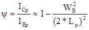 (6.5)
(6.5)
Than more vacant electron
sites is injected by the emitter in basis, than more them extract a collector,
augmenting a collector current. Therefore current ![]() is
proportional to an emitter current and is termed current controlled of a
collector, which in view of relations (6.3) and (6.5) is defined by a relation
(6.6) also records as follows:
is
proportional to an emitter current and is termed current controlled of a
collector, which in view of relations (6.3) and (6.5) is defined by a relation
(6.6) also records as follows:
![]() (6.6)
(6.6)
![]() - is termed as an integrated
(static) transmission factor current of emitter in a collector circuit and in
view of relations (6.3), (6,5) is defined by the following formula:
- is termed as an integrated
(static) transmission factor current of emitter in a collector circuit and in
view of relations (6.3), (6,5) is defined by the following formula:
 . (6.7)
Opportunity of control of an output current of the transistor by change entering current is the important property of the bipolar transistor, allowing to use it as a fissile device of electronic circuits.
Except for a controllable
part of a collector current ![]() , in an
electrode
, in an
electrode
collector the unguided part of
a current - thermal current backswitched of junction flows past. It is similar
to a current backswitched of a crystal diode and consequently has received a
title of a backward collector current ![]() .
.
index c means, that it - current backswitched of collector junction,
index b - the measurings occur in the circuit with CB,
index 0 - the measurings
occur at ![]() =0, i.e. No-load operation
on an input.
=0, i.e. No-load operation
on an input.
The direction of a
backward collector current ![]() coincides
with a direction of a controllable part of a collector current and consequently
coincides
with a direction of a controllable part of a collector current and consequently
![]() .
(6.8)
.
(6.8)
The current ![]() in a circuit of basis is
guided towards to a base current of a recombination
in a circuit of basis is
guided towards to a base current of a recombination ![]() and
base current of injection
and
base current of injection ![]()
![]() .
(6.9)
.
(6.9)
In an emitter circuit the
current of injection is the total of a collector current ![]() and base current
and base current ![]() :
:
![]() .
(6.10)
.
(6.10)
The expressions (6.8) and (6.10) establish communication between currents of the transistor and valid for any circuit of insert.
The similar processes occur in n-p-n the transistor to that by variance, that instead of vacant electron sites it is necessary to speak about electrons and on the contrary. Positive directions of direct currents and supply voltages, relevant to a fissile condition, are shown in a fig. 6.3.
Reverse voltage affixed on collector junction, it is much more voltages directly switched of emitter junction, and the currents are equal emitter circuits and collector practically. Therefore load power established variable component collector current, appears much more power expended on control by a circuital current of the emitter, hence transistor has intensifying properties. These qualities in a combination to a small overall dimensions, high reliability, longevity and profitability have stipulated wide application of transistors in an electron technology.
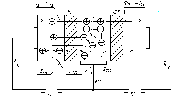
Fig. 6.4. Driving of carriers and currents in BT (fissile condition)
In the circuit with CE and CC (fig. 6.3) a current basises becomes control current, and the equation of a collector current (6.8) will be copied in the following aspect:
![]() ;
;
![]() ;
;
 . (6.11)
where: ![]() - transmission factor of a
base current in the circuit with CE:
- transmission factor of a
base current in the circuit with CE:
![]() - unguided part of a collector current in
the circuit with CE, or through current of the transistor.
- unguided part of a collector current in
the circuit with CE, or through current of the transistor.
For the circuit with CC an output current is the emitter current. Therefore
or
![]() ,where
,where![]() .
(6.12)
.
(6.12)
4. Inverse condition. In an inverse condition emitter junction backswitched, and the collector junction is under direct voltage. Therefore in comparison with a fissile condition in an inverse condition the injection of carriers is carried out collector junction, and extractions of carriers - emitter junction. Practically emitter and collector vary by functions and places in the circuit.
For the circuit with CB
![]() .
(6.13)
.
(6.13)
here ![]() - inverse coefficient of
transmission.
- inverse coefficient of
transmission.
As the area of emitter
junction is much less than the area collector junction and ![]() ,
, ![]()
For the circuit with CC
![]() .
(6.14)
.
(6.14)
For the circuit with CE
![]() .
(6.15)
.
(6.15)
6.3. Differential coefficient of transmission of a current
In the equation (6.7) for
an integrated (static) transmission factor of an emitter current ![]() . Coefficient of injection
. Coefficient of injection ![]() the efficiency of emitter
junction characterizes, and coefficient of diffusive transport
the efficiency of emitter
junction characterizes, and coefficient of diffusive transport ![]() characterizes processes in
basis, diffusive transport and recombination of carriers, with which attends
this process; coefficient M is inlet for the account of processes in collector
junction and almost always M=1. The equation of a collector current
characterizes processes in
basis, diffusive transport and recombination of carriers, with which attends
this process; coefficient M is inlet for the account of processes in collector
junction and almost always M=1. The equation of a collector current ![]() , where
, where ![]() is static parameter of
fissile condition of insert (fissile condition), displays link between direct
currents. Coefficient
is static parameter of
fissile condition of insert (fissile condition), displays link between direct
currents. Coefficient ![]() is defined by
the formula
is defined by
the formula ![]() and this formula displays
link between stationary values of a control current
and this formula displays
link between stationary values of a control current ![]() and
value of an output current
and
value of an output current ![]() .
.
For variable signals, which
amplitude order much less grades of supply voltages, link between collector
currents and emitter is defined by derivation of a relation (6.7) as functions
two arguments in the conjecture ![]() =const,
i.e.
=const,
i.e.
![]() , or
, or
![]() .
(6.16)
.
(6.16)
![]() - differential transmission
factor of an emitter current in circuit with CB, which always is more than
integrated coefficient
- differential transmission
factor of an emitter current in circuit with CB, which always is more than
integrated coefficient ![]() . Calculations display, that at major levels
of injection, when
. Calculations display, that at major levels
of injection, when ![]() (see of the
formula (6.1), (6.4)), derivative
(see of the
formula (6.1), (6.4)), derivative ![]() aspires
to zero and
aspires
to zero and ![]() . Therefore for the analysis of a major signal integrated
(static) coefficient
. Therefore for the analysis of a major signal integrated
(static) coefficient ![]() is always used.
is always used.
In consequent viewing is
not done variances between ![]() and
and ![]() . Using a label
. Using a label ![]() , but in
each case the applications of these magnitudes should be remembered a level of
injection.
, but in
each case the applications of these magnitudes should be remembered a level of
injection.
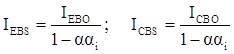
6.4. Ebers-Moll’s model
Links between currents and voltages in the transistor for four conditions of insert are well compounded with convenient and clear mathematical Ebers-Moll’s model, grounded on a dual circuit consisting of two diodes (emitter and collector), switched on meeting, and two current sources mapping interaction of these diodes (fig. 6.5).
![]() (6.17)
(6.17)
 .
(6.18)
.
(6.18)
where ![]() and
and ![]() - thermal currents emitter
and collector junctions accordingly, metered at short-circuit on exit and input
accordingly (
- thermal currents emitter
and collector junctions accordingly, metered at short-circuit on exit and input
accordingly (![]() =0 and
=0 and ![]() =0).
=0).
 .
(6.19)
.
(6.19)
where ![]() and
and ![]() - back currents of emitter
and collector junctions measured accordingly at abruption of a collector and
the emitter. With the account (6.18), (6.19) relations (6.17) are conversed to
an aspect
- back currents of emitter
and collector junctions measured accordingly at abruption of a collector and
the emitter. With the account (6.18), (6.19) relations (6.17) are conversed to
an aspect
 ;
(6.20)
;
(6.20)
 ;
(6.21)
;
(6.21)
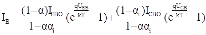 .
(6.22)
.
(6.22)
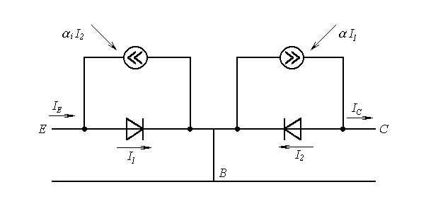
Fig. 6.5. Equivalent nonlinear Ebers-Moll’s model for BT
In computing methods of the analysis of transistor circuits with the help of a computer the wide circulation was received by nonlinear model of the Gummel-Pun’s transistor, which grounded on the solution of integrated relations for charges and links exterior electrical performances a charge in basis of transistor structure. It is very precise model explaining many physical effects, but its exposition needs major number of parameters, so for the analysis in a wide frequency range 25 parameters are necessary. The sequential simplification of Gummel-Pun’s model eventually reduces in the elementary Ebers-Moll’s model. Therefore at the analysis of the concrete circuits it is necessary to search for the reasonable compromise between an exactitude of the solution and complexity of model.
© 2009 База Рефератов